|
|


 Home > 제품소개 > Negative ebeam resist

- AR-N 7520 New - Negative E-beam Resist
- CharacterisationProperties
- E-beam, deep UV, i-line (formerly SX AR-N 7520/4).
- Short writing times, very high contrast.
- Mix & match processes between e-beam and UV exposure
248-365 nm, negative in the UV range.
- Highest resolution, very process-stable (no CAR).
- Plasma etching resistant, temp.-stable up to 140 °C.
- novolac, organic crosslinking agent.
- safer solvent PGMEA.Parameter /AR-N 7520 New .17 .11 .07 Thickness (μm) /4000 rpm 0.4 0.2 0.1 Resolution best value (nm) 28 Plasma etching rates (nm/min)
(5 Pa, 240-250 V Bias)Ar-sputtering 8 O2 169 CF4 41 80 CF4 + 16 O2 90 Spin CurveProcess chemicals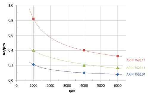
Adhesion promotor AR 300-80 Developer AR 300-47, AR 300-46 Thinner AR 300-12 Remover AR 600-71, 300-73 Process results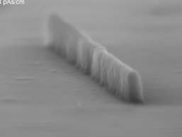 AR-N 7520.07 new 30-nm lines at a film thickness of 90 nm
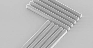 AR-N 7520.17 new 400 and 600 nm lines, thickness 400 nm
- Products Guide
* Double coating.ToneProduct (link)Film Thickness (nm)FeatureAdhesion Promoter SurPass series NA Apply resist: Novolac, DNQ, PMMA, HSQ, PMGI, SU-8, SML, PI, ... Negative ebeam resist HSQ series 8 – 1,650 Dilution: 1 - 45%.
Supply: Powder, Solution.H-SiQ series 25 – 850 Dilution: 2 - 20%.
Supply: Powder, Solution.AR-N 7520 New series 100 – 800 Best resolution: 28 nm.
e-beam, DUV, i-line.Positive ebeam resist HARP PMMA series 50 – 3,700 m/W: 950K, 495K.
Dilution: 2 - 11 %.HARP-C Copolymer series 150 – 1,100 MMA/MAA Copolyer.
Dilution: 6 - 12 %.PMMA series 40 – 7,000 m/W: 950K, 495K, 350K, 120K, 35K.
Dilution: 1 - 18 %.Copolymer series 100 – 1,100 Copolymer.
Dilution: 1 - 13 %.SML series 50 – 4,800 High resolution: 5 nm. Aspect ratio: >50:1.
Slow etch rate.Conductive layer DisCharge H2O series 25 – 170 Apply resist: PMMA, HSQ, mr-PosEBR, AR-P 6200, ZEP, SML. Protective Surface Coating PSC-1003 2.4 – 5.3 Protective Surface Coating PSC-IB DPM 1010 10 (@ 2000 RPM) Protective Surface Coating
![]()


엔엠테크 | 인천광역시 서구 가정로 437,110동 31층 2호 |
Tel : 070-8809-8665 |
팩스 : -
Copyright © 엔엠테크 All rights reserved.