|
|


 Home > 제품소개 > Negative photo resist

- XP 405nm NPR 2 - 405nm wavelength Negative Photoresist
- Sample DescriptionProcessing
- Straight wall negative photoresist in KemLab Inc NPR photoresist series modified for 405nm wavelength exposure.
- Lithography: Images look excellent under microscope: using a mask, 1 micron lines resolved withvery little LER.- Coat: Spread Cycle: 5 sec spread cycle at 1000 rpm, Spin Cycle: Accelerate at 1000 r/s to final spin speed for 45 seconds.
- Soft-Bake: 110o C for 90 seconds (hotplate)
- Exposure: Broadband contact exposure 300 mJ/cm2 at 405nm wavelength using 400nm cutoff filter on silicon. Intensity @ 405 = 18.4 mW/cm2.
- Dose will vary on different substrates & exposure tools. For single wavelength exposure tool, we think it will need ~ 50% more dose, but we have no way to measure.
- Post Exposure Bake: 110o C for 90 seconds (hotplate)
- Develop: ~ 30 - 40 seconds: immersion in 0.26N TMAH developer
- Film Thickness = 2.04 micron at 2000 rpm, Viscosity = 16 cst
Wavelength (nm)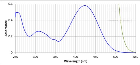
- Products Guide
-
* Double coating.ToneProduct (link)Film Thickness (µm)FeatureAdhesion Promoter SurPass NA Novolac, DNQ, PMMA, HSQ, PMGI, SU-8, SML, PI, ... Negative HARE SQ series 2 – 100 and 200* Epoxy. SQ QuickDry series 2 – 200 Epoxy, Quick drying solvent. SQ MicroCoat series 0.05 – 2 Epoxy, Thin film, Surface protection. SQ OptiCoat series 2 – 100 Epoxy, Higher transparency. APOL-LO 3200 series 2 – 10+ Lift-off profile. KL NPR series 1 – 20 Vertical profile. XP 405nm NPR 2 2 405nm wavelength exposure, Vertical profile. Image Reversal KL IR 15,
KL IR Lift-Off 151.2 – 2.6 Lift-off profile (negative),
Vertical profile (negative).Positive KL 7000 series 0.15 – 3 High resolution, No PFAS and Fluorine. KL 6000 series 2.5 – 11 General thick purpose. K-PRO series 0.8 – 25 and 50* Plating and etch application.
Advanced packagingProtective Surface Coating PSC-1003 2.4 – 5.3 Protective Surface Coating Conductive layer DisCharge H2OX4 80 – 170 Improved Scanning Electron Microscope
Imaging on Non-Conductive Substrate
![]()


엔엠테크 | 인천광역시 서구 가정로 437,110동 31층 2호 |
Tel : 070-8809-8665 |
팩스 : -
Copyright © 엔엠테크 All rights reserved.